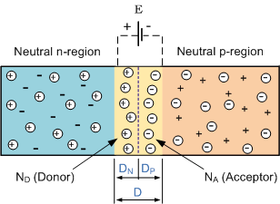
PN Junctions are important in semiconductors and electronics. P-type semiconductors with excess holes are joined to N-type semiconductors with excess electrons to make it. Controlling and manipulating current flow makes this junction essential for electronics applications. PN Junction behavior and features are crucial to studying and developing electrical devices like diodes and transistors.
What’s PN Junction?
A semiconductor material’s PN Junction is a boundary or interface between P- and N-type regions. Trivalent or pentavalent impurities are carefully doped into the semiconductor material to form the P and N regions. P-type regions have more holes, while N-type regions have more electrons. The diffusion and drift of charge carriers affect current flow across the PN Junction, giving it distinctive electrical features. Electronics requires knowledge of PN Junction structure and behavior.
Wondering what happens inside a diode, a tiny silicon piece? The mysterious PN junction powers those two-terminal electrical components that only allow one-way current flow. Do not be intimidated by the unusual terminology—PN junctions are the foundation of diodes and modern electronics. This beginner’s guide explains PN junctions, their importance, and how they’re made. By the end, PN junctions will seem like straightforward notions you can apply to any diode or semiconductor device rather than quantum bits. Ready to decipher the PN junction? Dive in.PN Junction Importance

PN Junctions are crucial to electronics and semiconductor devices. A key feature of PN Junctions is their ability to control current flow. Many electronic circuits employ them for rectification, switching, and amplification. Radios, TVs, and computers depend on PN Junctions, which form diodes, transistors, and integrated circuits. Understanding and using PN junctions is crucial to modern electronics.
Formation of PN Junction
We must first understand doping to comprehend PN junction formation. Doping an intrinsic semiconductor changes its electrical characteristics by adding impurities. Doping silicon with elements with one more or one less valence electron creates n- or p-type semiconductors.
On the boundary between n- and p-type semiconductors, intriguing things happen. Free electrons from n-type silicon diffuse into p-type silicon, where electron holes attract them. Also, p-type silicon holes permeate into n-type silicon, where free electrons fill them. Charge carriers diffuse across the connection, creating an initial diffusion current.
However, when more electrons and holes recombine across the junction, majority charge carriers decrease at the interface. Nearly no free charge carriers remain around the intersection. The depleted region generates an electric field that drives free electrons and holes in opposite directions, creating a drift current.
Drift and diffusion currents balance at equilibrium, thus no net current flows across the junction. The depleted zone grows until drift and diffusion currents balance. The final depletion zone comprises fixed donor and acceptor atoms ionized by charge carrier loss or gain. This area controls numerous PN junction features.
When forward biased, the PN junction conducts current in one direction and blocks current in the other. The PN junction is the foundation of diodes, bipolar junction transistors, and solar cells. Understanding its formation reveals its characteristics and uses.
PN Junction Features
Forward or backward biased PN junctions have different characteristics. Forward bias reduces depletion region width. Under reverse bias, it rises. See what occurs in each case.
Forward bias
Forward biasing the PN junction involves applying positive and negative voltages to the P- and N-type materials. This moves electrons and holes across the connection, narrowing the depletion region. N-type electrons go to the positive terminal and P-type holes to the negative terminal.
A narrower depletion region lowers resistance, enabling more current via the diode. Silicon diodes have a 0.7V forward voltage drop. Internal resistance raises voltage loss at larger currents.
The reverse bias
Reverse biasing the PN junction by applying positive and negative voltages to the P- and N-type materials widens the depletion zone. Electrons and holes leave the connection, widening the depletion region and increasing resistance. This causes a microampere reverse saturation current.
Diodes can be damaged by reverse voltages above the breakdown voltage. Doping concentrations and semiconductor material determine breakdown voltage. The majority of silicon diodes operate between 50 and 1000V.
In summary, PN junctions allow current flow when forward biased and prevent it when reverse biased. Understanding semiconductor diode operation requires understanding PN junction behavior in each bias mode.
Key PN Junction Uses
Many significant semiconductor devices are built around PN junctions. They enable daily-use diodes, transistors, photodiodes, and LEDs.
Current-rectifying diodes
Diodes allow current to flow in one direction via PN junctions. AC current is “rectified” into DC. electricity supplies convert AC wall electricity into DC power for electronics using diodes. Radios, TVs, and other gadgets detect and magnify radio frequency signals using them.
Switching and amplification transistors
Transistors switch and amplify electronic impulses via two PN junctions. They underpin all modern devices, including radios, TVs, smartphones, and computers. Transistors operate as amplifiers by controlling a large output signal with a small input signal. High-speed switches turn electronic circuits on and off.
Optical photodiodes and LEDs
PN junctions convert light to electricity in photodiodes and LEDs. Cameras, remote controllers, and smoke detectors employ photodiodes to convert light into an electronic signal. LEDs provide light when electric current runs through them, used in displays, flashlights, and more.
Due of its capacity to control electron and light flow, the PN junction powers many modern electronics devices. The special features of the PN junction allow diodes, transistors, photodiodes, and LEDs to amplify, switch, detect, and emit electrical and optical signals. PN junctions changed electronics and are now part of our daily lives.
Conclusion
That concludes a brief introduction to the PN junction, the building block of modern electronics. You now understand PN junctions, their formation, and their properties under forward and reverse bias. PN junctions power transistors, diodes, and integrated circuits, although their concepts are simple. You’ll design PN junction circuits quickly with practice. Next time you use your phone, computer, or other electronics, enjoy PN junctions. Demonstrate the PN junction to your friends so you may all marvel at its simplicity and power.

Leave a Reply